You know how Ampleon releases LDMOS devices rated at extreme power levels, like their ART2K rated at 2500W?
Unfortunately, that power rating really has nothing to do with linear use, which is what we need for amateur radio. That power rating is for a 100uS pulse at 108Mhz, with 75Vds, 50mA bias and 25C case temp.
This has little in common with a linear class AB amplifier for a mode like SSB. Kind of a ridiculous rating, for Amateur Radio anyway, since nothing linear can happen at 50mA bias and after the first pulse, you’re well above 25C.
So let’s talk about trying to run these amps as linearly as possible at the most common voltage out there, 50V.
By linear, I mean sine wave in, sine wave out, low harmonic content. Not a square wave output, or some other creative shape, caused by very strong harmonics. And, I’m talking pre-LPF, or no LPF.
Basically, what is the amplifier doing before the LPF cleaning crew has to come in and make everything ok.
900 Watts in a Perfect World
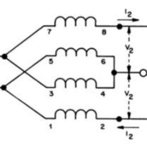
Let’s assume perfect components, including transistors that are linear and saturate at zero volts. In this case, each transistor can pull its drain down from 50V to 0V. And, when it pulls its drain low, the drain of the other transistor is pulled up by the same amount, beyond the 50V supply, by the perfectly coupled feed transformer, aka the CMFC.
Given that, each drain will swing between 0 and 100V. And while one drain is at 0, the other is at 100V, and vice versa. So a load connected between the drains sees from +100V to -100V. That’s a voltage of 200Vpp, or 100V peak, and since it’s a sine wave, that’s 70.7V RMS. If the transistors are driven any stronger, the tops of the sine wave will flatten, and you get distortion. So the 70.7V RMS is the largest signal the amplifier can produce without distortion, between the drains.
In my designs, this then goes into a 1:9 TLT. That’s 1:9 impedance ratio, meaning 1:3 voltage ratio. So the output voltage is 3×70.7V, and that’s 212.2V.
212.2V is the maximum possible RMS voltage at the output. And 212.2V, on 50Ω, makes 900W.
So that’s the theoretical/ideal limit for undistorted output power into 50Ω, at 50v, with 1:9 transformation, and perfect components throughout.
“Ignoring friction” as they used to say in engineering college.
From theoretical 900W to semi-reality 733W
Now let’s get more into the real world, where components are not perfect and CMFCs are FAR from perfect and do not behave as described above. And, there are other issues.
The first big issue is the MOSFETs cannot pull their drains fully down to zero volts.
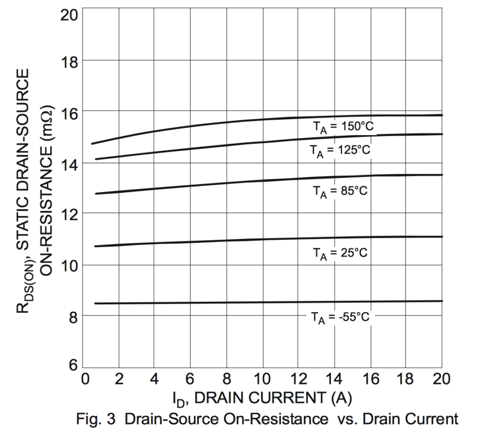
When the gates are driven as far as they will tolerate, the drain-source path at best has the resistance specified as RDS(on). This is roughly 0.08 to 0.16Ω for the typical kilowatt-class LDMOS. The lower value is valid at room temperature. When operating, they are much hotter, so this value grows, up to about twice the rated value. For a calculation, let’s assume a practical value of 0.15Ω.
Looking backwards now from the load, the 50Ω load impedance gets transformed to 5.5Ω by the 1:9 transformer, and that gets transformed to 1.39Ω by the 1:4 (2T) bifilar CMFC choke.
So, when the transistor is driven to saturation, the 50V supply is applied to a voltage divider consisting of 1.39Ω in series with 0.15Ω RDS(on). So the drain voltage only goes down to 4.9V instead of 0V causing the drain voltage excursions to reach only 45.1V up and down from the 50V supply. Therefore the max undistorted RMS voltage between drains is only 63.8V RMS, the output voltage is only 191.5V, and the max undistorted power output is only 733W.
This RDS(on) limitation is the primary limitation at low frequencies. But at higher frequencies there is an additional problem. The drain-source and drain-gate capacitances of a MOSFET tend to rise brutally when the drain voltage gets low, as the signal gets near zero.
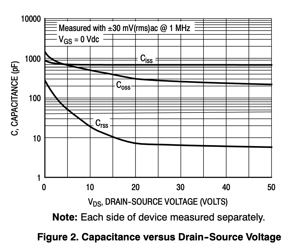
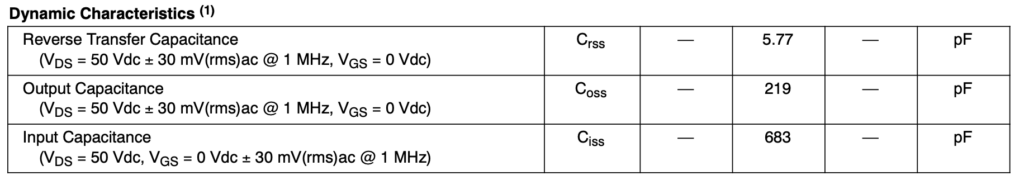
These rising capacitances cause a gain drop for big signals, and also cause phase distortion. The higher the frequency, the worse the effect. So, at high frequencies you can’t drive a MOSFET to its RDS(on)-dictated saturation voltage. As a result, the maximum undistorted power output gets even lower.
And there’s more..
Also, there are some more resistances in the circuit, which all contribute to reducing the output power even further. These effects should be small, but at least we can control them somewhat: short wide PCB traces, large sized coax cables, low ESR capacitors, etc.
Last, the typical CMFC is not capable of doing what we need at higher frequencies, say above 10Mhz. The coupling is far from perfect so the pulling up and down of the opposite side transistor via mutual inductance breaks down.
In Summary
In summary, at 50V, 733W is the theoretical max for linear operation and depending on frequency, this drops fast.
But don’t despair, because all you have to do is go non-linear and turn your sine waves into amplified square waves, which creates twice the power of a sine wave, and filter out the harmonics in a beefy LPF.
Just like all the big commercial amp makers do!
Leave a Reply