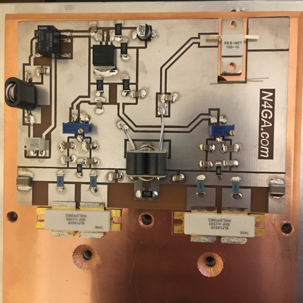
Designed this new little front end PCB this weekend.
My primary goals were as follows:
- Provide a regulated bias supply using a precision regulator to provide more accurate regulation and some ripple rejection, unlike a straight zener.
- Allow for independent adjustment of each LDMOS bias, with absolutely no interaction, i.e., adjustment to one side has zero affect the other side. The reason I want this is to be able to experiment with harmonic nulling.
- Incorporate a bias relay and 12V input conditioning onto the PCB, for less external components.
- Design a specific temperature compensated bias slope of -25mV/deg C using a common, highly accurate 3-pin adjustable voltage regulator.
- Incorporate a single flange type attenuator into the design for simplicity and lower cost.
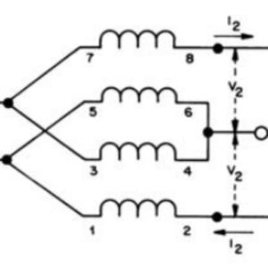
- Start working on normalization of gain, by first trying to neutralize the RF path post-attenuator through the 4:1 input transformer. First pass attempt here involves providing a termination resistor and trying to offset the capacitance in the transformer.
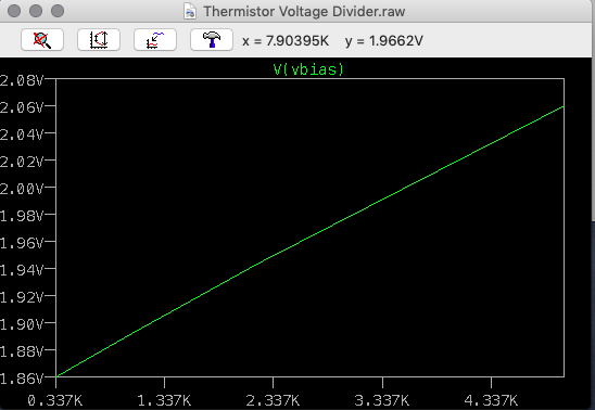
By far the largest point of interest here is #4. For this I set up SPICE simulations and ran Monte Carlo on resistance values in conjunction with a 2% 5k NTC thermistor, using the value curves from the manufacturer.
Simulating, I was able to come up with component values that produced exactly -25mv/C from 25C to 45C, then becomes steeper 45 to 65C, then steeper still 65C to 85C. Which I would think is ideal.
We’ll see how it all plays after I complete the redesign of the output board. This is much less involved, only dealing with mechanicals for now.


Leave a Reply